This section covers the technical standards for Displaytech monochrome LCD modules.
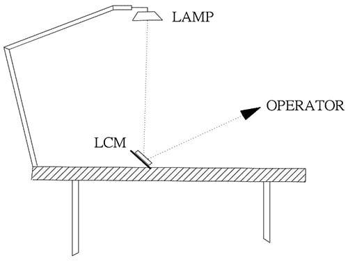
Inspection Condition
- Put the display under a lamp (20w x 2) at a distance of 100mm
- Tilt upright at a 45 degree angle by the front to inspect the LCD appearance
Image
AQL Inspection Level
Sample Method: MIL-STD-105D
Sampling Plan: Single
Major Defect: 0.65% (Major)
Minor Defect: 2.5% (Minor)
General Level: II / Normal
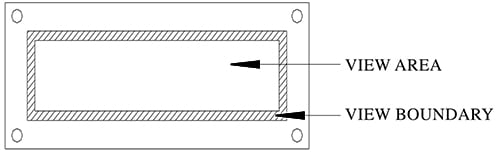
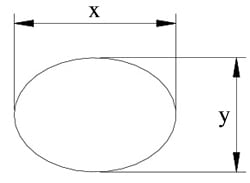
Display Area Definition
Image
LCD Inspection and Test Standard
Functional Test Standard
Acceptable Range
| Item | Inspection Standard Description | Standard | Defect Type | ||||||
|---|---|---|---|---|---|---|---|---|---|
| 1 | LCD Has No Display | Reject | Major | ||||||
| 2 | LCM Display Does Not Change | Reject | Major | ||||||
| 3 | Display Has Wrong Pattern | Reject | Major | ||||||
| 4 | Missing Segment on Display
Image

|
Reject | Major | ||||||
| 5 | Dim Segment on Display
Image

|
Reject | Major | ||||||
| 6 | Wrong LCD Viewing Direction | Reject | Major | ||||||
| 7 | Dim Display | See Sample | Major | ||||||
| 8 | LCD color variation | See Sample | Major | ||||||
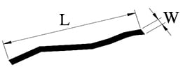
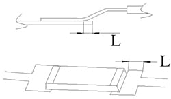
| 9 | Pattern Parallelism
Image
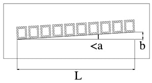
|
Acceptable Range | |||||||
| L | <a | b | |||||||
| ≧ 20mm | |0.43°| | ≦ 0.15mm | Accept | ||||||
| ≧ 30mm | |0.38°| | ≦ 0.2mm | |||||||
| ≧ 40mm | |0.43°| | ≦ 0.3mm | |||||||
| ≧ 50mm | |0.40°| | ≦ 0.35mm | |||||||
| ≧ 60mm | |0.43°| | ≦ 0.45mm | |||||||
| ≧ 70mm | |0.41°| | ≦ 0.50mm | |||||||
| ≧ 80mm | |0.43°| | ≦ 0.60mm | |||||||
| ≧ 90mm | |0.41°| | ≦ 0.65mm | |||||||
| ≧ 100mm | |0.43°| | ≦ 0.75mm | |||||||
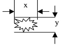
| 10 | LCD Display Pin Hole
Image
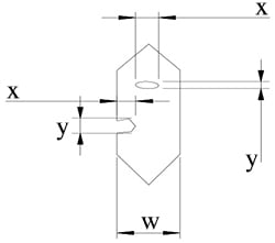
|
Standard | |||||||
| Ø = (x + y) / 2 | QTY | ||||||||
| Ø ≦ 0.25 | 1 | Accept | |||||||
| Ø > 0.25 | 1 | Accept | |||||||
| Ø < 1/4 W | 1 | Accept | |||||||
| Ø > 1/4 W | 1 | Reject | Minor | ||||||
| 11 | LCD Display Broken Segment (Dots) Image
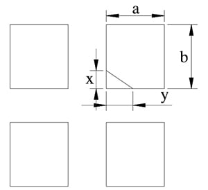
|
Standard | |||||||
| X | y | QTY | |||||||
| ≧ 1/4 b | ≧ 1/4 a | 1 | Reject | Minor | |||||
| (X or y) ≧ 0.2mm | 1 | Reject | Minor | ||||||
| ≦ 1/4 b | ≦ 1/4 a | 1 | Accept | ||||||
| ≦ 1/5 b | ≦ 1/5 a | 2 | Accept | ||||||
| 12 | LCD Display Black Spot or White Spot
Image
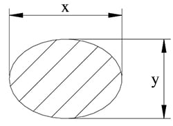
|
Ø = (x +y) / 2 | QTY | ||||||
| Ø < 0.10 | Accept | ||||||||
| 0.1 < Ø ≦ 0.20 | 2 | Accept | |||||||
| 0.20 ≦ Ø < 0.25 | 1 | Accept | |||||||
| 0.25 < Ø ≦ 0.4 | 0 | Reject | Minor | ||||||
| Ø > 0.4 | 0 | Reject | Major | ||||||
| 13 | LCD Display Excess Black Line or White Line | Black Line / White Line (L x w) mm | QTY | ||||||
| (L ≦ 1.0) × (W ≦ 0.025) | 2 | Accept | |||||||
| (1.0 < L ≦ 1.5) × (W ≦ 一 ‧ 0.025) | 1 | Accept | |||||||
| (L > 1.5) × (W ≦ 0.025) | 0 | Reject | Minor | ||||||
| (L > 2) × (W > 0.025) | 0 | Reject | Major | ||||||
| 14 | Backlight Does Not Function | Reject | Major | ||||||
| 15 | LED Does Not Function or Dim | Reject | Minor | ||||||
| 16 | Backlight Defect (dirt or scratch) | Reject | Minor | ||||||
Cosmetic Standard - LCD Appearance
| 1 | LCD Inspection Description | Standard | Defect Type | |||
|---|---|---|---|---|---|---|
| 1.1 | LCD Color Variation | See Sample | Minor | |||
| 1.2 | LCD Broken | Reject | Major | |||
| 1.3 | Wrong Polarizer of LCD | Reject | Major | |||
| 1.4 | Spot on LCD Surface | Reject | Major | |||
| 1.5 | Scratch on LCD Image
Ø = (x + y) / 2 |
Scratch = Ø | QTY | |||
| Ø < 0.1 | Except | Accept | ||||
| 0.1 ≦ Ø ≦ 0.15 | 2 | Accept | ||||
| 0.15 < Ø ≦ 0.25 | 1 | Accept | ||||
| Ø > 0.25 | 1 | Reject | Minor | |||
| 1.6 | LCD Scratch Depth Image
|
Scratch = L | Scratch = W | QTY | ||
| W ≦ 0.015 | Accept | |||||
| < 0.5 | W ≦ 0.02 | 2 | Accept | |||
| < 1.0 | W ≦ 0.03 | 1 | Accept | |||
| ≧ 1.0 | W ≧ 0.03 | 1 | Reject | Minor | ||
| 1.7 | White or Black Spot on LCD
Image
|
QTY | ||||
| Ø < 0.1 | Accept | |||||
| 0.1 ≦ Ø < 0.2 | 2 | Accept | ||||
| 0.2 ≦ Ø ≦ 0.25 | 1 | Accept | ||||
| Ø > 0.25 | 1 | Reject | Minor | |||
| Bevy point | - | Reject | Minor | |||
| 1.8 |
Black Line in LCD Image
|
(L) | (W) | QTY | ||
| L ≦ 1.0 | W ≦ 0.025 | 2 | Accept | |||
| 1.0 < 1 ≦ 1.5 | W ≦ 0.025 | 1 | Accept | |||
| 1.5 < L | W > 0.025 | 1 | Reject | Minor | ||
| 1.9 | Round Air Bubble | Size | QTY | |||
| Ø < 0.15 | 2 | Accept | ||||
| 0.15 ≦ Ø ≦ 0.25 | 1 | Accept | ||||
| Ø > 0.25 | 0 | Reject | Minor | |||
| 1.10 | Line Defect | (L) | (W) | QTY | ||
| L < 0.5 | W < 0.02 | 2 | Accept | |||
| L < 1.0 | W < 0.03 | 1 | Accept | |||
| L ≧ 1.0 | W ≧ 0.3 | 0 | Reject | Minor | ||
| 1.11 | Finger Print | Reject | Minor | |||
Cosmetic Standard - PCB / COB Appearance
| 2 | PCB/COB Specification Description | Standard | Defect Type | |||
|---|---|---|---|---|---|---|
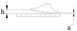
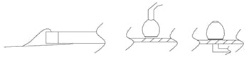
| 2.1 | PCB Deformity
Image
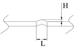
|
L | H | |||
| ≦ 6.0mm | ≦ 1.5mm | Accept | ||||
| > 6.0mm | ≦ 1.5mm | Reject | Minor | |||
| < 6.0mm | > 1.5mm | Reject | Minor | |||
| > 6.0mm | > 1.5mm | Reject | Minor | |||
| 2.2 | Deformity at PCB Edge, Damage Circuit | Reject | Major | |||
| 2.3 | Convex at PCB Edge
Image
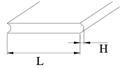
|
L | H | |||
| ≦ 6.0mm | ≦ 1.5mm | Accept | ||||
| > 6.0mm | ≦ 1.5mm | Reject | Minor | |||
| < 6.0mm | > 1.5mm | Reject | Minor | |||
| > 6.0mm | > 1.5mm | Reject | Minor | |||
| 2.4 | Damage Excess 2 x 2mm at the PCB Corner | Reject | Minor | |||
| 2.5 | Scratch on PCB Surface | See Sample | Minor | |||
| 2.6 | Scratch on PCB Coat / Leakage Coat on PCB Surface | Reject | Major | |||
| 2.7 | Open Circuit | Reject | Major | |||
| 2.8 | PCB PTH Open | Reject | Major | |||
| 2.9 | Repair PCB PTH | QTY ≦ 2PCS | Accept | |||
| QTY ≧ 3PCS | Reject | Major | ||||
| 2.10 | Color Different from One Side to Another Side | Reject | Minor | |||
| 2.11 | Repaired Solder Mask Area | ≦ 30mm2 | Accept | |||
| ≧ 30mm2 | Reject | Minor | ||||
| 2.12 | Scratch Circuit, Damage Circuit
Image
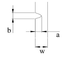
|
a ≦ 1/2w or b < w | Accept | |||
| a > 1/2w or b > w | Reject | |||||
Cosmetic Standard - Bezel Appearance
| 3 | Bezel Specification Description | Standard | Defect Type | ||||
|---|---|---|---|---|---|---|---|
| 3.1 | Wrong Materials | Major | |||||
| 3.2 | Incorrect Dimensions | Major | |||||
| 3.3 | Bezel Broken | Major | |||||
| 3.4 | Rust on Bezel | Major | |||||
| 3.5 | Hole or Dirty on Oil Paint Surface | Size | cm2/per | ||||
| Top Surface | Ø ≦ 0.3 | 2 | Accept | ||||
| 0.3 < Ø ≦ 0.5 | 1 | Accept | |||||
| Ø > 0.5 | 0 | Reject | Minor | ||||
| Side | Ø ≦ 0.5 | 2 | Accept | ||||
| 0.5 < Ø ≦ 0.8 | 1 | Accept | |||||
| Ø > 0.8 | 0 | Reject | Minor | ||||
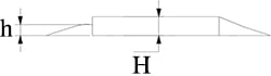
| 3.6 | Bezel Bow or Twist | h ≦ 0.01 mm/mm | Accept | ||||
| h > 0.01 mm/mm | Reject | Minor | |||||
| 3.7 |
Image
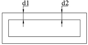
|
d1 - d2 ≦ tolerance | Accept | ||||
| d1 - d2 > tolerance | Reject | Minor | |||||
| 3.8 | Scratch on Bezel
Image
|
Face | Accept QTY | ||||
| L | W | Not Defined | See Sample | ||||
| - | W ≦ 0.15 | ||||||
| L ≦ 3 | W ≦ 0.20 | 2 | |||||
| L ≦ 2 | W ≦ 0.3 | 2 | |||||
| - | W > 0.3 | ||||||
| Side | Accept QTY | ||||||
| L | W | ||||||
| - | W ≦ 0.2 | except | See Sample | ||||
| L ≦ 3 | W ≦ 0.25 | 2 | |||||
| L ≦ 2 | W ≦ 0.3 | 2 | |||||
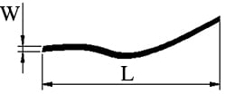
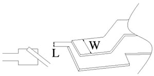
| 3.9 | Twist Angle α = 45º + 5º
Image
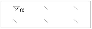
|
Accept | |||||
| 3.10 | Void Gap Between Bezel and PCB | Reject | Minor | ||||
| 3.11 | Bezel Clip Incorrectly
Image
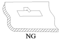
|
Reject | Minor | ||||
Cosmetic Standard - Solder
| 4 | Solder Specification Description | Standard | Defect Type | ||||
|---|---|---|---|---|---|---|---|
| 4.1 | Wrong Component | Reject | Major | ||||
| 4.2 | Broken Component | Reject | Major | ||||
| 4.3 | Misalignment
Image
|
Component legs extend beyond the pad and Legs > pad distance (w) on solder area > W2 | Accept | ||||
| Component legs extend beyond the pad and Legs > pad distance (w) on solder area < W2 | Reject | Minor | |||||
| Component Offset
Image
|
Solder legs offset distance L < 1/4W | Accept | |||||
| Solder legs offset L > 1/4W | Reject | Minor | |||||
| 4.4 | Component Assembly Defect
Image
|
Reject | Minor | ||||
| 4.5 | CHIP Components Hoist ≦ 0.5mm | Accept | |||||
| 4.6 | CHIP Components Hoist > 0.5mm | Reject | Minor | ||||
| 4.7 | Components Hoist | h ≦ 2.0mm | Accept | ||||
| h > 2.0mm | Reject | Minor | |||||
| 4.8 | Switch (socket) Hoist | h ≦ 0.5mm | Accept | ||||
| h > 0.5mm | Reject | Minor | |||||
| 4.9 | Components Cold Solder or Incomplete Solder | Reject | Major | ||||
| 4.10 | Solder PAD Tilted Up, but Height (h) is less than Solder PAD thickness (a)
Image
|
Accept | |||||
| 4.11 | Excess Solder Above Components
Image
|
Reject | Minor | ||||
| 4.12 | Insufficient Solder Below Components Height or less than Diameter
Image
|
Reject | Minor | ||||
| 4.13 | Solder Area less than Soldering PAD Area by 2/3 | Reject | Minor | ||||
| 4.14 | Trimmed Pin Length Beyond 0.09 inch (2.3mm)
Image
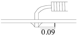
|
Reject | Minor | ||||
Packaging Standard
| 5 | Packaging Specification Description | Standard | Defect Type |
|---|---|---|---|
| 5.1 | Wrong Carton Mark | Reject | Major |
| 5.2 | Carton Mark Issue | Reject | Minor |
| 5.3 | Carton Damage Extends more than 150mm | Reject | Major |
| 5.4 | Carton Damage or Scratch is more than 50mm but less than 150mm | Reject | Minor |